The multi-functional scanner fluorescence imaging system is a high-precision instrument that uses laser precision scanning, time-resolved acquisition and image processing techniques to obtain the photophysical properties of materials in the micro-nano scale space. It is mainly used to study the fluorescence kinetic process and imaging in the micro and nano scale of semiconductor samples, photoelectric conversion materials, photocatalytic materials and biological samples. Its main structure includes laser light source, microscope (ortho or inverted), laser scanning device and detector, etc. It can be fully automated, digital image acquisition and processing through computer control, and can realize various imaging and detection functions such as fluorescence intensity confocal imaging, fluorescence lifetime imaging, carrier migration imaging, micro-nano space fluorescence spectroscopy and Raman spectroscopy acquisition. The system can also be combined with low-temperature device, high-voltage device, (transient) photocurrent/photovoltage detection device and pulse voltage device to achieve a variety of external field conditions of fluorescence kinetics detection, high spatial resolution of photocurrent imaging, electroluminescence kinetics and imaging and other special functions.

06Application Example 2: Carrier Migration Dynamics Imaging
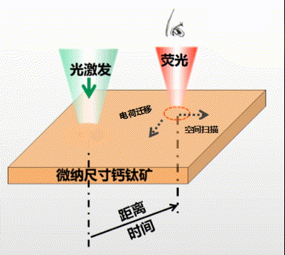
Imaging principle: The system adopts laser fixed-point excitation and fluorescence acquisition vibrational field scanning mode, which can realize the visual imaging of the material planar-scale carrier migration (diffusion) kinetic process. The detection mode introduces excitation light (not through the vibrational field) through the rear port of the microscope and selects a specific location to excite the sample, while the fluorescence acquisition channel passes through the vibrational field into the detector. During the imaging process, the position of the excitation point is kept constant, and the scanning of the vibrational field enables the fluorescence to be collected at different locations on the sample surface. Based on the migration of photogenerated carriers in the migration of composite luminescence characteristics, the above imaging mode can realize the carrier migration from the excitation position to other positions of the sample kinetic process, to achieve the most intuitive imaging detection. The kinetic process of carrier migration can be reflected by the time information (TCSPC acquisition) and distance information (vibroseis pixel distance) between the acquisition point (vibroseis pixel position) and the excitation point. By fitting the fluorescence kinetic process, the carrier migration coefficient, carrier complex time (lifetime) and carrier migration distance can be simultaneously obtained for micro- and nano-sized samples (or within the sample micro- and nano-sized space).

Working principle diagram
Working principle animation demonstration
Sample: Calcium titanium oxide nanowires
Imaging mode: carrier migration dynamics imaging


Time-sharing imaging map
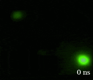
Realize dynamic visual imaging
The spatial distribution of the fluorescence intensity of chalcogenide nanowires is obtained in fixed excitation-fluorescence scanning mode, in which the fluorescence intensity I(t)x,y at any position (x,y) of the sample at time t is proportional to the carrier concentration (φ(t)x,y) at that position at time t.

Therefore, this fluorescence imaging map reflects the change of carrier concentration distribution in the nanowire at different moments, and this evolution process reflects the carrier migration from the excitation point (high concentration) to the unexcited region (low concentration) of the nanowire driven by the concentration gradient, and the information of carrier mobility, lifetime and migration distance can be obtained by extracting the fluorescence dynamics curves at different positions and fitting, and also by data analysis software The fluorescence imaging map of nanowires at different moments can also be obtained by data analysis software, and a very intuitive dynamic evolution of fluorescence intensity can be constructed.
Reference:
W. Tian, C. Zhao, J. Leng, R. Cui, S. Jin*. J. Am. Chem. Soc., 2015, 137, 12458-12461
Sample: Calcium titanite polycrystalline film
Imaging mode: carrier migration dynamics imaging

Fixed-point excitation fluorescence acquisition scanning imaging and fixed-point extraction kinetics
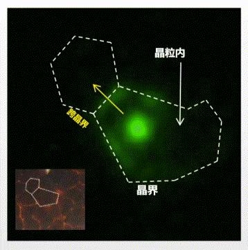
►Probing carrier migration dynamics in complex polycrystalline structures
► Carrier migration within and across grains can be observed
(Note: limited by grain size)

Imaging of surface charge extraction efficiency in chalcogenide polycrystalline films; Spiro-OMeTAD: hole acceptor; PCBM: electron acceptor
Reference:
W. Tian, et al., T. Lian*, S. Jin*. Angew. Chem. Intl. Edit. 2016, 55, 13067-13071.
07Application example 3: Fluorescence spot diffusion imaging

Based on the fixed excitation-fluorescence scanning imaging mode, the carrier migration kinetic parameters are obtained by collecting and analyzing the changes of fluorescence spot size at different moments after excitation.
►Applicable to short-range carrier migration material systems
► Spatial resolution of migration distance can be achieved: ~50 nm
Sample: CS2AgBiBr6 calcium titanite
Imaging mode: fluorescence spot diffusion observation carrier migration dynamics imaging

Larger spot size


References
YanfengYin,WenmingTian,*etal.JimingBian.andShengyeJin,ACSEnergyLett.2022,7,154-161
Sample: Calcium titanium oxide thin film
Researchers have successfully probed the effect of passivation of different polymer materials on the surface of chalcogenide solar cells and its enhancement of carrier mobility coefficient using this system


Reference:
Minhuan Wang, et al. Rational selection of the polymeric structure for interface engineering of perovskite solar cells, Joule, 2022.
08Application example 4: Fluorescence imaging in a cryogenic chamber
The fluorescence imaging system can be combined with a microscope cryogenic device, and according to the parameters of the cryogenic device, the objective lens with different working group distances can be selected to achieve efficient acquisition of fluorescence information. Various imaging and data acquisition such as fluorescence intensity, fluorescence lifetime, carrier migration and fluorescence emission spectrum can be performed at different temperatures.
Sample: MAPbI3 nanowires
Experimental conditions: 100X, spatial resolution < 1μm
Imaging mode: Confocal laser scanning imaging mode


Observation of the spatial distribution and evolution of the low-temperature phase transition process of chalcogenide nanoprecursors
09Application example 5: Fluorescence imaging in an autoclave
The fluorescence imaging system can be combined with a high voltage device for microscopy, and according to the parameters of the high voltage device, the objective lens with different working group distances can be selected to achieve efficient acquisition of fluorescence information. Various imaging and data acquisition such as fluorescence intensity, fluorescence lifetime, carrier migration and fluorescence emission spectrum can be performed at different temperatures.
Sample: MAPbI3 single crystal nanosheets and MAPbI3 nanowires
Experimental conditions: 100X air mirror, spatial resolution < 1μm
Imaging modes: Confocal laser scanning imaging mode and carrier migration imaging mode

Laser scanning fluorescence imaging of MAPbI3 nanowires under different pressures

Fluorescence kinetic curves at different pressures

Fluorescence imaging of carrier migration in MAPbI3 nanowires under different pressures

Carrier migration kinetic curves at different pressures
References: YanfengYin,WenmingTian,*etal.,JimingBian.andShengyeJinACS Energy Lett.2022,7,154-161
10Application example 6: Electroluminescence kinetic imaging

This fluorescence imaging system enables electroluminescence (EL) kinetic and imaging detection of samples (e.g. LED devices or materials) by combining an electric pulse generator, which is compatible with the detection of fluorescence intensity, fluorescence lifetime and fluorescence/EL emission spectra simultaneously. The detection principle is to use TCSPC technology to realize the kinetic evolution process of sample luminescence and EL spatial imaging under electric pulse conditions.
Sample: CdSe/ZnSe/Zns quantum dot LED devices
Voltage: 10V
Pulse width / frequency: 10μs/10KHz


► The EL distribution of the LED emitting layer can be observed, and the bad spot areas that exist can be found.
► Observe the difference and variation of EL dynamics and overshoot phenomenon in different micro-nano area points by extracting EL dynamics
► Observation of LED aging process by continuous acquisition of EL imaging
11Application example 7: Photocurrent imaging
The fluorescence imaging system can be compatible with the detection of fluorescence intensity, fluorescence lifetime and fluorescence emission spectrum at the same time by combining the source meter to realize the sample (solar cell or photoelectric detection material) photocurrent imaging, micro and nano space I-V curve and other acquisition and imaging. The detection principle is to scan the laser spot on the sample through the vibration field and collect the photocurrent or other photoelectric parameters.
This system enables photocurrent and fluorescence imaging directly on the actual solar cell device

Working principle diagram


Direct imaging of device conditions
►The spatial structure of cell grains and grain boundaries and the photocurrent distribution between different grains can be clearly distinguished
►Compatible with acquisition of fluorescence intensity and fluorescence lifetime imaging to analyze the photocurrent generation mechanism
Large range imaging


Reference:
Zhao, X.; Wang, Z.; Tian, W.; Yan, X.; Shi, Y.; Wang, Y.; Sun, Z.; Jin, S., A positive correlation between local photocurrent and grain size in a perovskite Solar cell. Journal of Energy Chemistry 2022.
Source: Tristar Spectrum @ WeChat
Time: 2022/05/10