Micro and Nano Processing | 3D Optical Structure Grayscale Lithography
Grayscale processing techniques enable a variety of micro-optical elements for different applications. Both diffractive and refractive micro-optical elements can be processed using contour lithography forming methods and graphic etching transfer techniques. The more commonly processed micro-optical elements include beam-splitting diffractive optics, beam-forming diffractive elements, diffractive optics for scattering or uniform light distribution, diffractive lenses and lens arrays, refractive micro-lenses and micro-lens arrays (MLA), and other phase-modulated optical elements. The above-mentioned functional micro-optics for applications in the electromagnetic spectrum range have been fabricated on various substrate materials, and micro-optics for applications in the optical radiation spectrum range from DeepUltraviolet (DUV) with a wavelength of 157 nm to Long-WaveInfrared (LWIR) with a wavelength of 14 μm. LWIR) at a wavelength of 14 μm.
Grayscale lithography is achieved by fabricating a photomask such that the intensity of light radiation transmitted through the mask varies with spatial location. Several methods are available for this purpose, including photomasks with spatially varying optical density, photomasks with spatially varying light absorption, and the use of variable-size microstructured masks to modulate the light flux transmitted locally within the mask range. techniques belonging to the first category of grayscale lithography and graphic etching transfer techniques for fabricating micro-optical components were developed by Gal et al. The grayscale processing technique applies a single photolithography reaction process to etch the desired micro-optical 3D structure pattern on the photosensitive polymer.
The use of grayscale lithography gives designers greater freedom in solving micro-optical problems by combining positive (convex) and negative (concave) surfaces in the same optical element. Photoresists formed from grayscale can produce anamorphic objectives or "saddle" shaped lenses with positive or negative curvature along the orthogonal axis, and can form saddle shaped refractive surfaces to correct for image scattering wave fronts. Aspherical objectives and parabolic lenses, as well as micro-optical elements that perform multiple functions on a single optical surface, such as focusing and beam splitting, can be very easily fabricated using grayscale processing. The application of grayscale lithography has produced non-traditional optical elements, among which are phase-surface micro-optical lenses such as phase diffusers, beam integrators (or beam integrators), gratings, or spot generators.
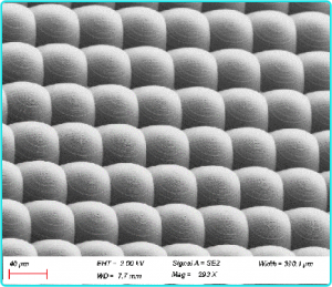
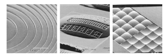
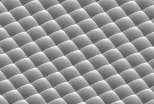
Examples of some common micro-optical structures fabricated by grayscale lithography are shown in Figure 1.1, including: smooth Kaino (phase holographic) diffractive lenses, micro-optical elements with both focusing and beam splitting functions on the same optical surface, and positive and negative MLAs with high fill factors. reactive ion etching (RIE) techniques can be applied to permanently transfer the characteristic contours of lithographic patterns onto the substrate surface. Reactive etching pattern transfer methods can utilize capacitively coupled etching devices or high-density plasma devices, including Inductively Coupled Plas-ma (ICP) etchers. In the field of microelectronics, the more desirable plasma etching techniques have been modified to enable successful etching of wafers including functional micro-optical devices, and the industry standard plasma etching processes used for oxide materials, silicon and compound semiconductors have been improved to make them suitable for processing micro-optical structures for transfer onto the various substrate materials mentioned above.

Figure 1.1 SEM images of typical micro-optical elements processed using the grayscale processing process (including diffractive lenses, micro-optical elements with both focusing and beam splitting functions, and convex and concave micro-lens arrays)
We offer fastMEMS device / micro and nanostructure processing design services, Feel free to leave a message to inquire.
Related Products
Related Reading
Micro and Nano Processing | Thin Film Preparation - PVD
Thin Film Preparation - PVD The most common physical methods used to date are
Micro and Nano Processing | Thin Film Preparation - Epitaxy
Thin Film Preparation - Epitaxy Most materials are amorphous, crystalline or polycrystalline in shape.
Micro and Nano Processing | MEMS Fine Processing (IV)
Micro and Nano Processing | MEMS Fine Processing (IV) 1.3 Photolithography


