Micro and Nano Processing | Thin Film Deposition, Lithography and Etching Overview
Nanofabrication is divided into three different areas: thin film, photolithography and etching.
Thin films, physical vapor deposition methods such as vapor deposition; sputtering; and pulsed laser and chemical vapor deposition are reviewed for low-pressure CVD, plasma-enhanced CVD, and atomic layer deposition (CVD).
Lithography, first discussing the principles of contact-mask lithography, then ultraviolet (UV) projection lithography, and finally more advanced systems for integrated circuit fabrication, such as deep-UV 193 nm and immersion lithography systems. Resolution enhancement techniques such as double patterning and self-aligning patterning are briefly reviewed. Non-optical lithography, such as electron beam lithography, focused ion beam lithography, and nanoimprint lithography, are also discussed.
Etching, topics include techniques used in wet chemical etching, plasma etching and deep silicon etching.
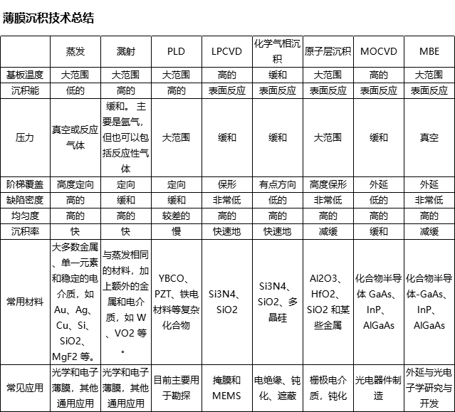
Thin Film Deposition Technology Summary
| Evaporation | Sputtering | PLD | LPCVD | Chemical Vapor Deposition | Atomic layer deposition | MOCVD | MBE | |
| Substrate temperature | Large Scale | Large Scale | Large Scale | High | moderate | Large Scale | High | Large Scale |
| Deposition energy | Low | High | High | Surface reaction | Surface reaction | Surface reaction | Surface reaction | Surface reaction |
| Pressure | Vacuum or reaction gas | Mild. Primarily argon, but can also include reactive gases | Large Scale | moderate | moderate | Large Scale | moderate | Vacuum |
| Step Coverage | Highly oriented | Oriented | Oriented | conformal | A little direction | Highly conformal | Extent | Extent |
| Defect Density | High | moderate | moderate | Very low | Low | Very low | Low | Very low |
| Uniformity | High | High | less favourable | High | High | High | High | High |
| Deposition rate | Quick | Quick | slow | Quickly | Quickly | Slow down | moderate | Slow down |
| Commonly used materials | Most metals, single elements and stable dielectrics, such as Au, Ag, Cu, Si, SiO2, MgF2, etc. | Same material as evaporation, plus additional metals and dielectrics such as W, VO2, etc. | YBCO, PZT, ferroelectric materials and other complex compounds | Si3N4, SiO2 | Si3N4, SiO2, polycrystalline silicon | Al2O3, HfO2, SiO2 and some metals | Compound Semiconductor GaAs, InP, AlGaAs | Compound semiconductors-GaAs, InP, AlGaAs |
| Common Applications | Optical and electronic films, other general purpose applications | Optical and electronic films, other general purpose applications | Currently used mainly for exploration | Masks and MEMS | Electrical insulation, passivation, masking | Gate dielectric, passivation | Optoelectronic device manufacturing | Epitaxy and Optoelectronics Research and Development |
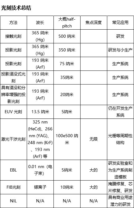
Lithography Summary
| Methods | Wave length | About half-pitch | Depth of Focus | Common Applications |
| Contact lithography | 365 nm (Hg) | 500 nm | Research and Development | |
| Projection lithography | 365 nm (Hg) | 350 nm | R&D and small production | |
| Projection lithography | 193 nm (ArF) | 75 nm | Production System | |
| Projection immersion lithography | 193 nm (ArF) | 35nm | Production System | |
| Projection lithography with immersion and resolution enhancement | 193 nm (ArF) | 20nm | Production System | |
| EUV lithography | 13.5 nm | 5nm | Production systems still being developed | |
| Laser Interference Lithography | 325 nm (HeCd), 266 nm (YAG), 248 nm (KrF), 193 nm (ArF), etc. | 100e500 nm | Infinite | Periodic structures such as grids |
| EBL | 0.01 nm (electron beam) | 5nm | Large | R&D lab and manufacturing templates for production systems |
| FIB lithography | Gallium ion | 10nm | Large | Mask repair, chip repair, R&D |
| NIL | N/A | N/A | N/A | R&D with potential for commercial use |
The Half-pitch values given here are the actual values of these systems, not their theoretical limits.
Extended Reading.
- Micro and Nano Processing | Photolithography - Nanoimprint Lithography
- Micro and Nano Processing | Lithography - Focus on Ion Beam FIB
- Micro and Nano Processing | Lithography - Electron Beam Lithography
- Micro and Nano Processing | Photolithography - Optical Lithography
- Micro and Nano Processing | Etching
- Micro- and Nanofabrication | Thin Film Preparation - Epitaxy
- Micro and Nano Processing | Thin Film Preparation - PVD
- Micro and Nano Processing | Thin Film Preparation - CVD
We offer fastMEMS device / micro and nanostructure processing design services, Feel free to leave a message to inquire.

