
Introduction to microlens array丨Preparation and processing methods and applications
Catalog
What is a microlens array?
Microlens array (MLA) is an array of several microlenses with micron aperture and relief depth in a specific arrangement. By adjusting the shape, focal length, arrangement structure and duty cycle of the microlenses in the microlens array, certain optical functions can be realized and the integration and performance of the optical system can be improved. According to the different principles of beam modulation, they can be divided into diffractive microlenses and refractive microlenses.
The idea of the lens array originated from the compound eye structure in bionics. The visual system of the compound eye of animals in nature has been systematically studied since the early 20th century. The compound eye of the housefly consists of about 4,000 small eyes, and the small eye surfaces in the compound eye are generally hexagonal in shape, which can act as tiny optical units. It was inspired by the structure of compound eye path that Lippmann in France proposed the concept of microlens array in 1908.

Common materials used for microlenses
The first step in the microlens design and fabrication process is the selection of materials for making microlenses. Commonly used materials include polydimethylsiloxane (PDMS), polymethyl methacrylate (PMMA), photoresist, silicon dioxide (SiO2), etc.
- Polydimethylsiloxane (PDMS, polydimethylsiloxane)It is a silicone-containing thermosetting polymer with low surface energy and hydrophobicity, exhibiting good mechanical and thermal properties at high temperatures while providing a good surface finish. Moreover, it prevents the polymer from sticking to the mold surface during the separation process, which helps to release the mold. And the original PDMS has good transmittance in the visible region (400-700 nm) with higher transmittance than 93%. Since PDMS has good elasticity, flexibility, stability and optical properties. Therefore, PDMS can be used as an embossing mold for manufacturing various polymer microlenses, especially in the hot embossing method. Due to its good elasticity, flexibility, stability and optical properties, PDMS has been widely used in soft lithography to make elastomeric molds
- Polymethyl methacrylate (PMMA,polymethyl methacrylate)PMMA is the most excellent transparent thermoplastic polymer material, with light transmittance up to 92%, high transparency and brightness, good heat resistance, and good toughness. It also has the advantages of low cost, high mechanical strength, and easy processing. It is often used as a replacement material for glass. When heated at a temperature higher than the glass transition temperature, PMMA exhibits good plasticity and can be processed for hot embossing. By adjusting to the proper embossing temperature, a complete cavity filling can be achieved. In addition, PMMA has some applications in microlens manufacturing methods such as inkjet printing and energy beam direct writing.
- PhotoresistUnder certain wavelength of ultraviolet radiation, a reaction will occur to complete the solid state conversion. Photoresist is characterized by high sensitivity, high curing degree and fast curing speed. It is widely used in inkjet printing and photoresist thermal reflow for microlens manufacturing. SU-8 negative photoresist is a promising material for microlens fabrication because of its high transmittance, high refractive index and low polymer volume shrinkage in the visible to near-infrared range. SU-8 also has good mechanical properties, thermal stability and optical properties, making it suitable for the fabrication of micro-optical components.
Key parameters affecting the imaging of microlens arrays
Filling factor The height reflects the high utilization of the incident light by the microlens array. The larger the value, the higher the transmission rate of the microlens array, the more light energy reaches the image surface and the smaller the loss.
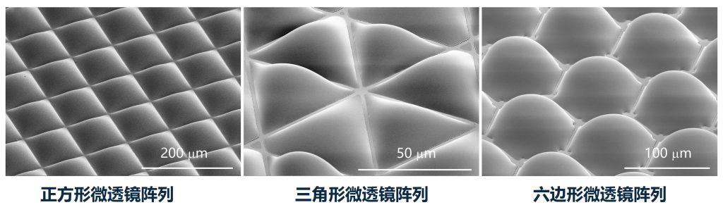
Shape/profile
Lens shapes: spherical, aspherical, cylindrical, non-cylindrical, free-form, toroidal, mini-Fresnel, deformed or biconical
Single-sided (plano-convex and plano-concave) or double-sided (double-sided convex, double-sided concave or concave-convex)
Curvature
Curvature affects focal length and NA
Microlens array preparation and processing method
| Microlens array fabrication method | Advantages | Disadvantages | Microlens diameter | |
| Direct method | Nano Thermal Imprinting Technology | Easy to operate Low cost High precision Suitable for large-scale preparation | Difficult to create templates Expensive equipment | ~500 μm |
| Microdrop injection process (Inkjet printing) | Simple processing Low cost Can be made on flexible substrates Suitable for large-scale preparation | Low numerical aperture Difficult to control size and surface shape | 50-100 μm | |
| Electric fluid power spray printing (E-jet-printing) | High surface smoothness High processing efficiency Flexible and reliable manufacturing process | Satellite droplets will form if the voltage is unstable | ~5 μm | |
| Self-assembly method | Easy to produce Good imaging performance Large area preparation | Difficult to maintain consistency | ~200 μm | |
| Thermal reflow method (Photoresist hot melt method) | Simple production process Low cost Short cycle time High efficiency Easy control of process parameters | Higher heating temperature required Difficult to control the geometry and uniformity of the lens Low numerical aperture | 30-200 μm | |
| Laser-based manufacturing methods (electron beam direct writing, focused ion beam direct writing, femtosecond laser, two-photon polymerization 3d printing, etc.) | High Resolution High flexibility | High process complexity Long processing cycle Expensive equipment | ~10 μm | |
| Indirect method | Wet Etching | High surface smoothness Good uniformity Good repeatability | Expensive equipment Mask preparation required | 5-60 μm |
| Soft lithography | Controllable shape Suitable for large area preparation | Templates to be prepared Complex and expensive to produce | ~445 nm | |
Application of microlens arrays
Microlens arrays are most commonly used to improve the light collection efficiency of charge-coupled device arrays. They collect and focus light that would otherwise fall on non-sensitive areas of the CCD. Microlens arrays are also commonly used in digital projectors to focus light. There are also combinations of microlens arrays designed for new imaging features, such as the ability to display images at unit magnification without image inversion. Microlens arrays are also used in compact imaging devices, such as smartphone cameras. Or they can be used in optical microscopes, where two arrays can be used to achieve uniform illumination. Finally, microlens arrays are also used to enable light field photography (all-optical cameras) so that images can be captured without initial focusing. Instead, focus is achieved during post-processing of the image using software.
Today, microlens arrays are becoming an integral part of most optical systems. The applications they are used for include.
- Confocal Microscope
- Digital Projector
- Display and HUD Imaging Systems
- Lighting System
- Lidar Systems
- Light field cameras and systems
- Medical Laser Systems
- Optical Sensors
- White light interferometer
We offerMicrolens arrays / Nanoimprinting / Micro and nanostructure processing design services, Feel free to leave a message to inquire.

