Introduction to super-surface lenses (metalenses) 丨Design principles, applications and processing methods

Catalog

What is a superlens?

Superlenses (Metalenses) are also known as superconfiguration lenses. It is a two-dimensional planar lens structure consisting of a super-surface (a planar two-dimensional (2D) lens with sub-wavelength thickness). Metamaterials) made of optical elements that focus light. It is touted as one of the top 10 emerging technologies for 2019.
With the advantages of thinner size, lighter weight, lower cost, better imaging, and easier integration, superlenses offer a potential solution for compact and integrated optical systems. And the properties of polarization, phase and amplitude of light can be tuned by adjusting the shape, rotation direction, height and other parameters of the structure.

The design principle of superlens and phase regulation method

The design principle of the hyperlens is based on two special features of the hypersurface.Selection of super-surface phase distribution and geometric design of nanoscale structures. Control of the optical wave properties (including phase, amplitude and polarization) can be achieved through the design and fabrication of geometric structures to adjust the profile, position and angle of the subwavelength structures, thus controlling the focusing and imaging characteristics of the superlens.
 
There are three basic phase modulation methods for superlenses.
Resonant phase modulation, propagation phase modulation, and geometric phase modulation (also known as PB phase modulation).
 
  • Resonance phase controlIt is the phase abrupt change by changing the resonant frequency, which is controlled by the geometry of the nanoscale structure. However, because resonant phase hypersurfaces are usually made of metal materials such as gold, silver, and aluminum, they inevitably cause ohmic losses and make it difficult to achieve high-efficiency optical field modulation. And the super-surface lens made of low-loss dielectric material can effectively solve this problem.
  • Propagation phaseis due to the fact that electromagnetic waves produce optical range differences during propagation, and phase modulation can be achieved by using this property. The phase regulation (φ) is regulated by the optical range difference, where the wavelength is λ , the effective refractive index of the medium is n, and the electromagnetic wave propagates at a distance d (the height of the structure) in a uniform medium, where k0=2π/λ is the free space wave vector, then the accumulated propagation phase of the electromagnetic wave can be expressed as
When the micro- and nanostructures are highly fixed, they can be adjusted by the shape, size and structural unit period of the micro- and nanostructures. Superlenses designed based on the propagation phase principle are usually composed of isotropic micro- and nanostructures with a high degree of symmetry. Therefore, they are endowed with hyperlens polarization insensitivity, i.e., the phase response of the micro- and nanostructures is independent of the polarization type of the incident light, and are suitable for most application scenarios.
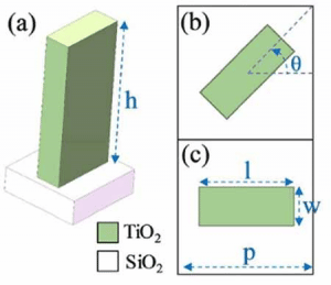
  • Geometric Phasesis an artificial control of phase gradients or distributions by adjusting the rotation angle of micro and nano structures with the same dimensions to achieve abrupt phase changes of optical waves, thus greatly reducing the complexity of designing and processing hypersurfaces. The advantage of geometric phase modulation is that it is not affected by material dispersion, structure size, and structural resonance.
 
In order to achieve the focusing lens function so that all light rays reach the same focal point, the phase of the planar superlens should satisfy.
where λ is the wavelength, f is the focal length, and x and y are the spatial coordinates relative to the center of the hyperlens. The phase corresponding to each position can be calculated, and the hyperlens is designed by realizing such a phase distribution through the hypersurface.
The cell rotation angle θ should satisfy the equation
 
The basic phase modulation principles for each of the three superconfiguration surfaces were introduced earlier; however, any phase modulation alone cannot achieve achromatic imaging or full-color imaging. In practical applications, a mixture of two or more principles is usually used to achieve phase modulation when making superlenses.

Current Research Status and Applications of Superlens

High numerical aperture (NA) superlenses

The focusing efficiency of a superlens is critical for imaging and sensing applications. The focusing efficiency of a superlens can be improved by suppressing 1) scattering caused by structures with wavelength-scale dimensions, 2) reflection caused by impedance mismatch, and 3) material absorption caused by material loss. Resonance, geometry, and propagation phase mechanisms can be used to enhance focusing performance.


Achromatic Superlens (AML)

As a diffractive optical device, superlenses, like other diffractive lenses, suffer from severe chromatic aberrations of their own. Although these lenses can operate in a wide range of optical wavelengths, the existence of chromatic aberration severely limits the application in optical focusing and imaging. Especially for optical super-resolution planar superconfiguration lenses, there are many challenges to eliminate chromatic aberrations in planar superconfiguration lenses while achieving super-resolution point optical diffusion.

  • Multi-wavelength achromatic superlenses based on low-loss coupled rectangular dielectric resonators
  • Broadband achromatic superlenses: building blocks and intensity distribution of different superlenses
  • Narrow-band achromatic superlens


Multifocal Superlens

A focusing lens with multiple focal points is an important optical element. In multispectral cameras, the use of multiple lenses to achieve multiple points of focus leads to large size, weight and high cost of the equipment. Supersurfaces can effectively solve this problem through specialized designs that can simplify the structure of optical systems with thinness, miniaturization, and high integration.
 

Superlens processing method

Based on photolithography

Photolithography is a process that combines exposure and etching. A mask with a designed pattern is placed on a substrate coated with photoresist. Under the irradiation of a specific light source, the photoresist is chemically modified. After development and etching, micron- and nanometer-scale graphic layers are formed on the substrate. The photolithography process typically includes substrate processing, substrate coating, rotational photoresist coating, soft drying, exposure, development, hard drying, etching, and testing.
Photolithography has high resolution and allows precise control of the shape and size of the formed pattern. It has a wide range of applications in semiconductor and microelectronics manufacturing, optics, biology, and metamaterials. However, its application is limited by the high cost of equipment, the high requirements of the environment in which it is used, and the limited availability of suitable materials.
 
Electron beam lithography (EBL)
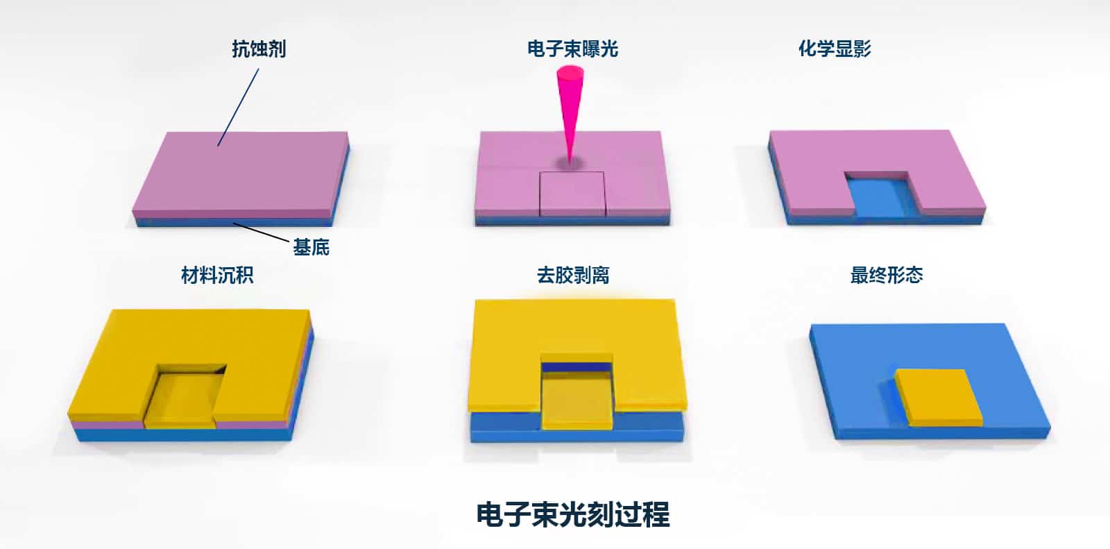
Utilizing an electron beam, a design pattern is written directly onto a resist-covered surface by changing the solubility of the resist. E-beam lithography is the highest resolution photolithography known, with a resolution of 10 nm or less. It has the advantage of ultra-high resolution and eliminates the need for a photolithographic mask plate.
 
The disadvantages are:
1, the exposure speed is slower forLess efficient and more time-consuming than large-area superlens production 
2. High preparation costs.Expensive equipment with high maintenance costs and consumables used in the process (e.g., e-beam photoresists) are also more expensive, leading toDifficult to apply large scale mass production .
Therefore, it is mostly used in the production of optical projection lithography templates, design and verification of new lithography technologies, experimental research, and prototyping.


Femtosecond Laser Direct Writing Lithography
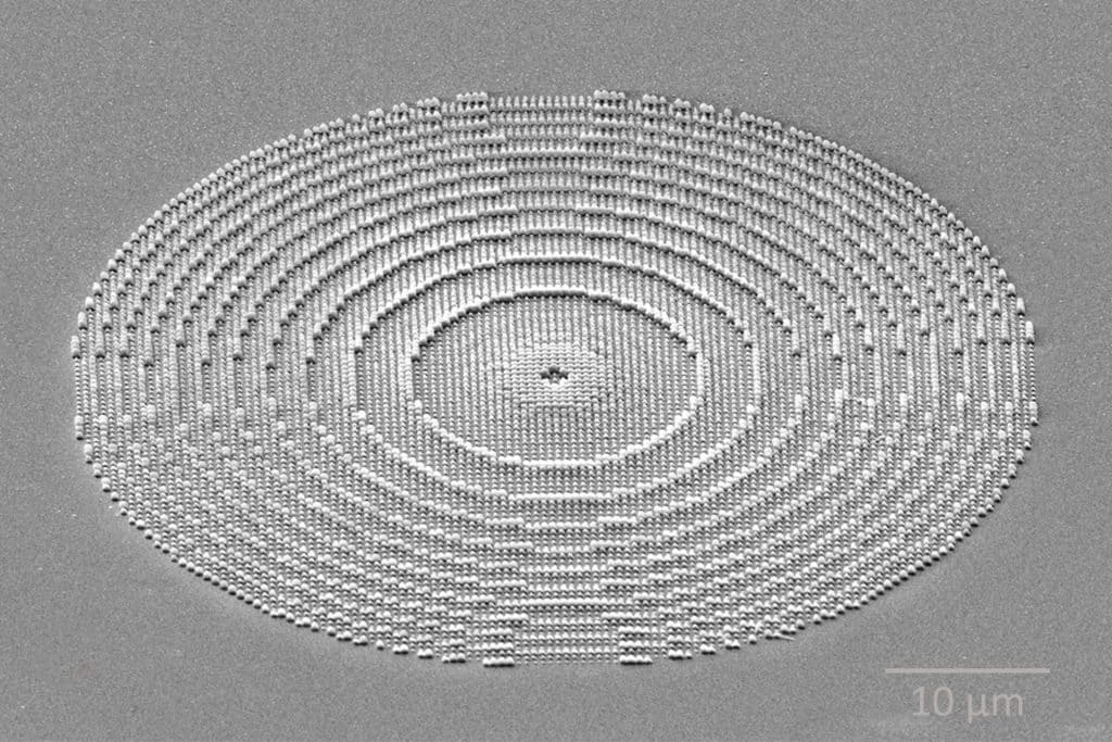
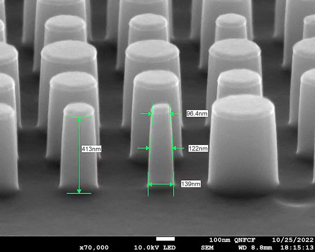
Femtosecond laser direct writing lithography, also known as two-photon lithography or two-photon polymerization (TPP), refers to the formation of micro/nanostructures by controlling the movement of the laser focus by focusing the femtosecond laser beam inside the light-sensitive material and initiating a polymerization reaction through a photoinitiator. Femtosecond lasers haveHigh precision, high flexibilityandTrue 3D processingWith the features such as the ability to fabricate precise 3D microstructures of arbitrary shapes without the need for optical masks, the smallest feature size can now reach 10 nm.

Superlens made with TPP technology


Nanoimprinting technology (in-depth knowledge)

Nanoimprintlithography (NIL) is a micro and nano-processing process to produce nanoscale patterns. It is a micro and nano process in which a template with a nanoscale pattern is applied to a polymer substrate in a certain way to replicate the pattern with equal scale embossing.
Nanoimprinting is the most common method for processing polymer structures. HavingLow cost, short lead time, high output, high resolutionThe advantages of the product include
The main mature and commonly used nanoimprinting technology processes are.Nano thermal imprinting (T-NIL) technology, UV-curable imprinting (UV-NIL) technology, and micro contact printing (μCP).

We offer Superstructured Lens / Micro and Nano Structures Processing Design Service, Feel free to leave a message to inquire.

Related Products

Related Reading