
Thin Film Deposition丨Atomic Layer Deposition (ALD)
Technology Principle and Application
Catalog
What is Atomic Layer Deposition (ALD)?
Atomic Layer Deposition (ALD) is a high precision chemical vapor deposition (CVD) based process. Thin Film Deposition TechnologyThis is a technique for depositing material materials in the form of single-atom films based on chemical vapor phases layer by layer on the substrate surface. Two or more precursor chemicals, each containing a different element of the material being deposited, are introduced one at a time onto the substrate surface. Each precursor saturates the surface to form a monolayer of material.

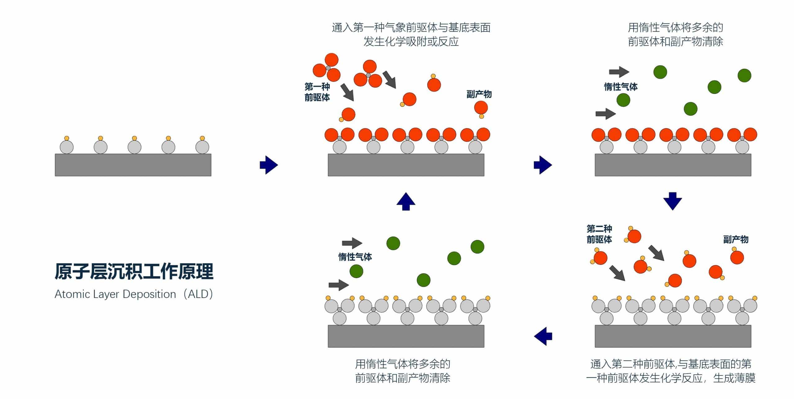
Principle of atomic layer deposition
The growth principle of ALD is similar to conventional chemical weather deposition (CVD), but in ALD, the reaction precursors are deposited alternately during the deposition process, and the chemical reaction of the new layer of atoms is directly associated with the previous layer, with only one layer of atoms deposited per reaction. Having self-limiting growth characteristics allows the film to be deposited onto the substrate conformally and without pinholes. ThereforeThe number of deposition cycles can be controlled to achieve precise control of film thickness.
An atomic layer deposition cycle can be divided into four steps.
- The passage of the first precursor gas into the substrate, theAdsorption or chemical reaction with the substrate surface.
- Flushing the remaining gas with inert gas.
- The introduction of a second precursor gas.Chemical reaction with the first precursor gas adsorbed on the surface of the substrate to produce the coating, or continued reaction with the products of the reaction between the first precursor and the substrate to produce the coating.
- Flush out the excess gas with inert gas again.
Precursor selection and classification
The choice of precursors plays a crucial role in the quality of the coating for ALD growth, and precursors need to meet.
- A sufficiently high vapor pressure at the deposition temperature to ensure that it can adequately cover the surface of the filled substrate material.
- Good thermal and chemical stability, preventing autolysis within the limits of the maximum temperature of the reaction.
- High reactivity. Rapid adsorption and saturation on the material surface, or rapid and effective reaction with the material surface groups
- Non-toxic, non-corrosive, and inert by-products Avoid hindering self-limiting film growth
- Wide range of material sources
ALD precursors can be divided into two main categories: inorganic and metal-organic. The inorganic precursors include monomers and halides, and the metal organics include compounds such as metal alkyl, metal cyclopentadienyl, metal β-2 ketone, metal amide, and metal ether groups.
Atomic layer deposition technology features and advantages
- High accuracy.The thickness of the substrate can be easily and precisely controlled by controlling the reaction cycle, and the thickness of the film can be as accurate as the thickness of an atom.
- Excellent three-dimensional conformability.ALD can produce a film with the same shape as the original substrate, i.e., the film can be deposited uniformly on a concave-like surface . ThereforeSuitable for different shapes of substratesUniform three-dimensional films, consistent shape and originality, and conformability are the unique advantages of ALD technology.
- High flatness.The pinhole-free surface, bottom-up growth mechanism determines the pinhole-free nature of the film, which is valuable for blocking and passivation applications.
- Excellent adhesion.Chemical adsorption of precursors to the substrate surface ensures excellent adhesion
- Low thermal budget (low precipitation temperature): Thin film growth at low temperatures (room to 400°C), which is attractive for temperature-constrained polymer devices and biomaterial coatings
Comparison of advantages and disadvantages of thin film deposition processes
| Craftsmanship | Atomic layer deposition (ALD) | Physical Vapor Deposition (PVD) | Chemical Vapor Deposition (CVD) | Low Pressure Chemical Vapor Deposition (LPCVD furnace tube) |
|---|---|---|---|---|
| Deposition principle | Chemical surface saturation Reaction-Deposition | Evaporation-Consolidation | Gas phase reaction - deposition | Low Pressure Chemical Vapor Deposition (Stove and tube type) |
| Deposition process | Laminar growth | Nucleation growth | Nucleation growth | Nucleation growth |
| Step coverage | Excellent | General | Good | Good |
| Deposition rate | slow | Quick | Quick | slower |
| Deposition temperature | Low(<500℃) | Low | High | Higher |
| Uniformity | Excellent 0.07 - 0.1nm | General About 5nm | better 0.5 - 2nm | Better |
| Thickness control | Number of reaction cycles | Deposition time | Deposition time Gas phase partial pressure | Deposition time Gas ratio |
| Ingredients | Uniformity with few impurities | No impurities | Easy to contain impurities | No impurities |
Atomic Layer Deposition Applications
As the semiconductor industry continues to evolve, the increasingly fine size of devices makes it particularly important to find or develop more advanced thin film growth techniques that require low thermal budgets, high film thickness accuracy and excellent conformality on three-dimensional (3D) structures, however, the traditional deposition techniques, chemical vapor deposition (CVD) and physical vapor deposition (PVD) are no longer fully adapted to this trend. ALD technology has a wide potential for applications in the fields of micro and nano electronics and nanomaterials due to its high controllability of deposition parameters (thickness, composition and structure), excellent homogeneity and conformality.
- The main areas of application of this technology include the following [1]:
- High K dielectric(Al2O3, Hf O2, Zr O, Ta 2 O5, La 2 O3): for transistor gate and DRAM capacitor dielectric layer;
- Metal grid electrode (Ir, Pt, Ru, Ti N);
- Metal Interconnects and Liners(Cu, WN, Ta N, WNC, Ru, Ir): Metal diffusion barrier layer for copper interconnects, semiconductor vias for transistor grids, and memory cell applications such as DRAM capacitors, passivation layers;
- Catalytic Materials(Pt, IrCo, Ti O2, V 2 O5): for coatings inside filter membranes, catalysts (platinum membranes for automotive catalytic converters), ion exchange coatings for fuel cells;
- Nanostructures (various materials): for conformal deposition around and inside nanostructures and MEMS;
- Bio-coatings(Ti N, Zr N, Cr N, Ti Al N, Al Ti N): Biocompatible materials for medical devices and instruments used in vivo;
- ALD Metal Materials(Ru, Pd, Ir, Pt, Rh, Co, Cu, Fe, Ni);
- Piezoelectric layer(Zn O, Al N, Zn S);
- Transparent electrical conductor(Zn O: Al, ITO);
- UV blocking layer(Zn O, Ti O2);
- OLED Passivation(Al2O3 );
- Solid lubrication layer(WS2);
- Photonic Crystals(Zn O, Zn S: Mn, Ti O2, Ta2 N5): inner coating of porous alumina and reverse opal;
- Anti-glare and optical filters(Al2O3 , Zn S, Sn O2, Ta 2 O5): Fabry-Perot trigger filter;
- Electroluminescent devices(Sr S: Cu, Zn S: Mn, Zn S: Tb, Sr S: Ce);
- Processing layer(Al2O3, Zr O2): used for etching potential barrier layer, ion diffusion potential barrier layer, coating of electromagnetic recording heads;
- Optical Applications(Al Ti O, Sn O2, Zn O): used in nano-optical materials, solar cells, integrated optical materials, optical thin films, lasers, various dielectric film making;
- Sensors(Sn O2, Ta 2 O5): for gas sensors, pH sensors;
- Wear and corrosion inhibiting layer (Al2O3 , Zr O2, WS2)
[1] Current status of application and development prospects of atomic layer deposition technology; (2021) 10-0005-05
We offer Atomic Layer Deposition / Micro-Nanofabrication Services, Feel free to leave a message to inquire.

