Micro-Nano Processing | Introduction and Application of Nanoimprinting (NIL) Technology
What is nanoimprinting technology?
Nanoimprint lithography (NIL) is a micro and nano process that uses a template with a pattern of micro and nano structures to transfer the pattern onto a corresponding substrate to create a nano-scale pattern, usually on a very thin polymer film, and is the most common processing method for processing polymer structures. HavingLow cost, short lead time, high output, high resolutionThe advantages of the product include
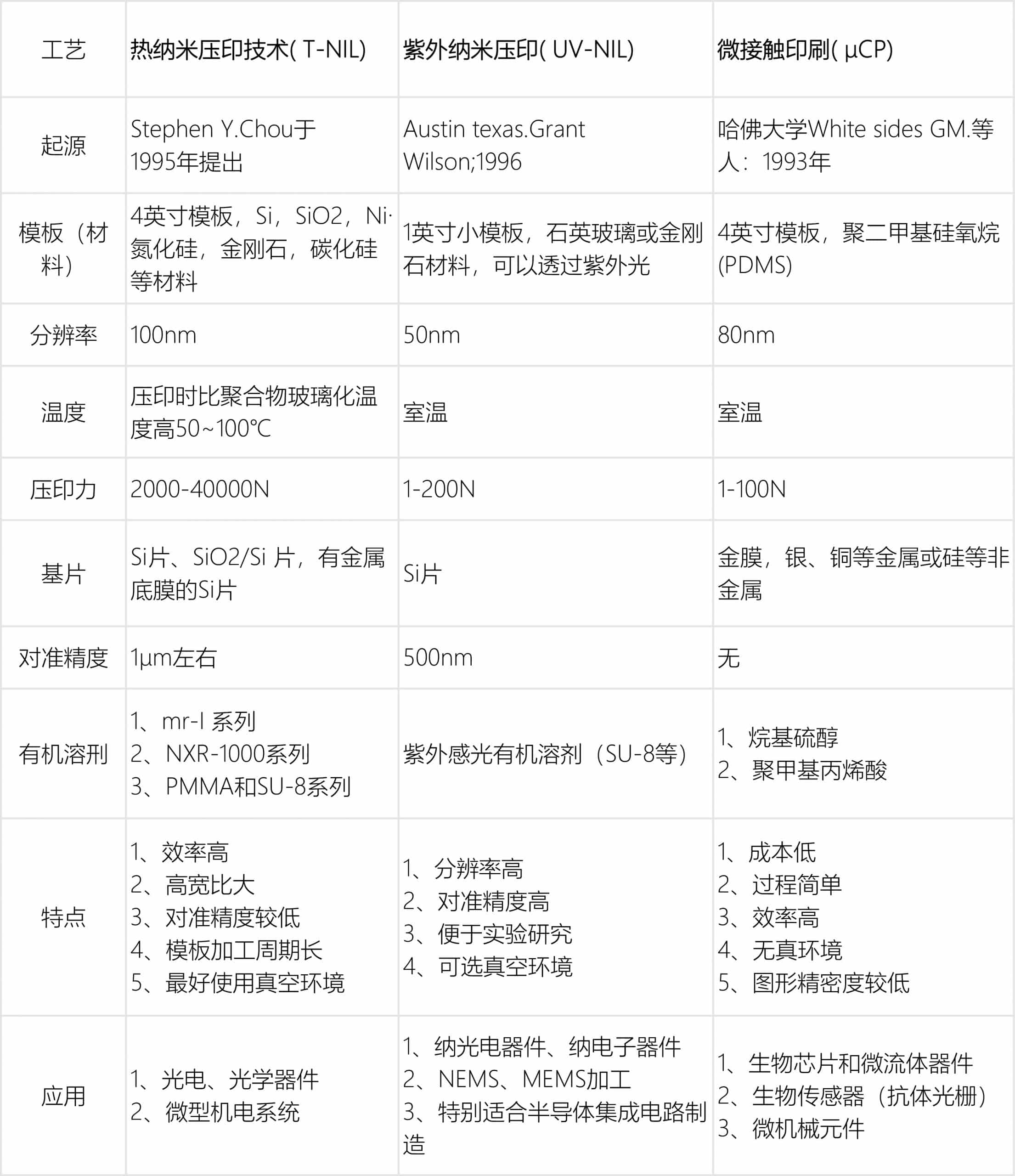
The main mature and commonly used nanoimprinting technology processes are.Thermal Nanoimprinting (T-NIL) technology, UV-curable imprinting (UV-NIL) technology and micro contact printing (μCP).
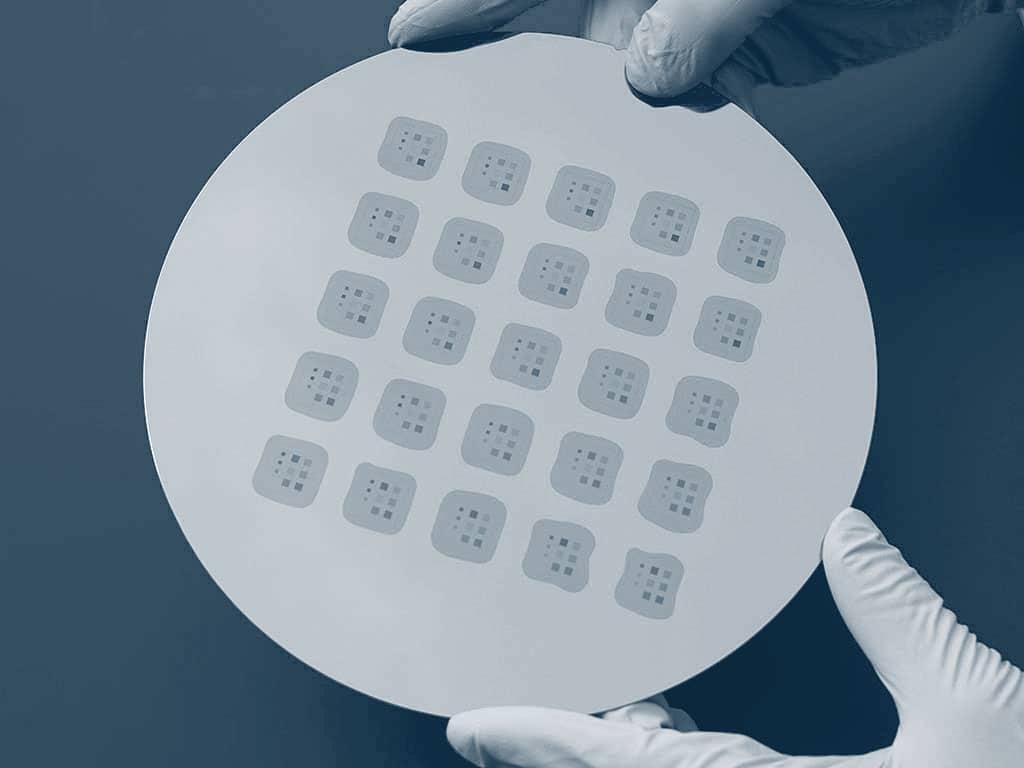
Nanoimprinting principle
The nanoimprinting process consists of three main steps.1、Graphic template preparation 2、Graphic copy 3、Graphic transfer
A polymer coating (e.g., polymethyl methacrylate, polystyrene, polycarbonate, etc.) is pre-attached to a silicon or other substrate as a substrate, and the template with the nano-pattern already engraved on it is contacted with the substrate and precisely embossed and shaped by the corresponding equipment and apparatus, and after certain conditions (e.g., time, pressure, temperature, light, etc.), the template is separated from the substrate so that the pattern can be reproduced and The nanostructure pattern on the template surface is transferred to the polymer coating on the substrate surface. Subsequently, the nanostructure patterns on the polymer coating are transferred to the substrate by using etching or peeling techniques to achieve the transfer of nanostructure patterns.
Introduction of various nanoimprinting processes
- Nano Thermal Imprinting Process (T-NIL)
The standard nano-thermal imprinting process (T-NIL) involves spin-coating a thin resist (thermoplastic polymer) onto a sample substrate, then contacting a template with a predefined topological pattern to the sample and pressing them together under a certain pressure. WhenPolymers areHeat toAbove the glass transition temperature, the pattern on the template is pressed into the softened polymer film. After allowing to cool, the template is separated from the sample and the pattern resist is left on the substrate. The pattern in the resist can be transferred to the substrate below using a pattern transfer process (reactive ion etching).
- Ultraviolet light curing embossing ( UV-NIL)
Unlike nanoimprinting, UV-curable imprinting (UV-NIL) is a room temperature imprinting technique in which a light (UV)-curable liquid resist is applied to a sample substrate, usually with a template made of a transparent material such as quartz or PDMS. after pressing the template and substrate together, the resist is cured under UV light and becomes solid. After the template is separated, the pattern in the resist can be transferred to the underlying material using a similar pattern transfer process.
- Micro Contact Printing (μCP)
Microcontact printing technology, also known as soft embossing technology, uses electron beam or optical lithography to create graphics on polydimethylsiloxane (PDMS) compared to the rigid stencil used in thermal and UV embossing, and then uses the patterned PDMS as a stencil for embossing and then performs the embossing process through the principle of molecular self-assembly.
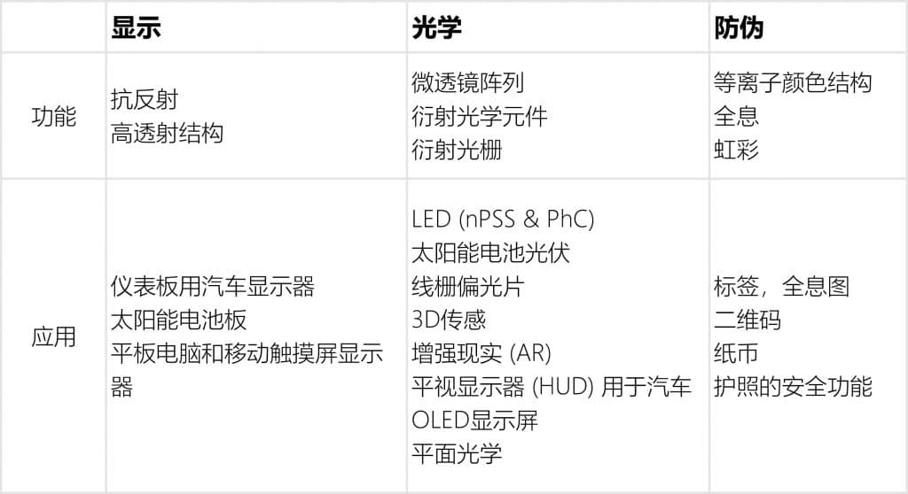
Application of nanoimprinting technology
We offerNanoimprint Stencil / Nanoimprint Reproduction / Micro-Nanostructure Processing Design Service, Feel free to leave a message to inquire.
Related Products
Related Reading
Micro and Nano Processing | Preparation of Micro and Nano Optical Components
微纳加工 | 制备微纳光学元件 微纳光学
Introduction to microfluidic chips丨Common materials and preparation and processing methods
Introduction to microfluidic chips丨Common materials and preparation and processing methods
Micro and Nano Processing | MEMS Micro Energy System Preparation
Micro and Nano Processing | MEMS Micro-Energy Device System Preparation

