Introduction to microfluidic chips丨Common materials and preparation and processing methods
Catalog
What is a microfluidic chip?
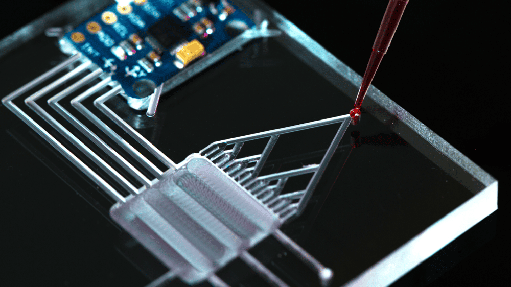
Microfluidics chip, also known as Lab-on-a Chip (LOC), is a chip that allows precise manipulation of minute amounts of fluid in micron-scale microtubes to perform various functions of conventional physical, chemical, or biological experiments on a micron-scale chip.Microfluidic microarrays have become a powerful tool for studying biological systems at single-cell resolution. At the same time, microfluidic chips can be widely used not only for manipulating microdroplet generation, microfluidic diffusion sieving and detection of protein-ligand interactions, but also for implementing molecular assays in biochemistry.
The micro-nano-fluidic chip has many advantages, such asHigh degree of automation, high efficiency, high throughput, miniaturization, low cost and ultra-low reagent consumptionIn particular, the precision of fluid manipulation can reach nanoliter (nL) and even femtoliter (fL) accuracy in the precise manipulation of micro and nano fluids, and thus has great potential for research in many interdisciplinary fields such as biology, medicine, physics, and chemistry.
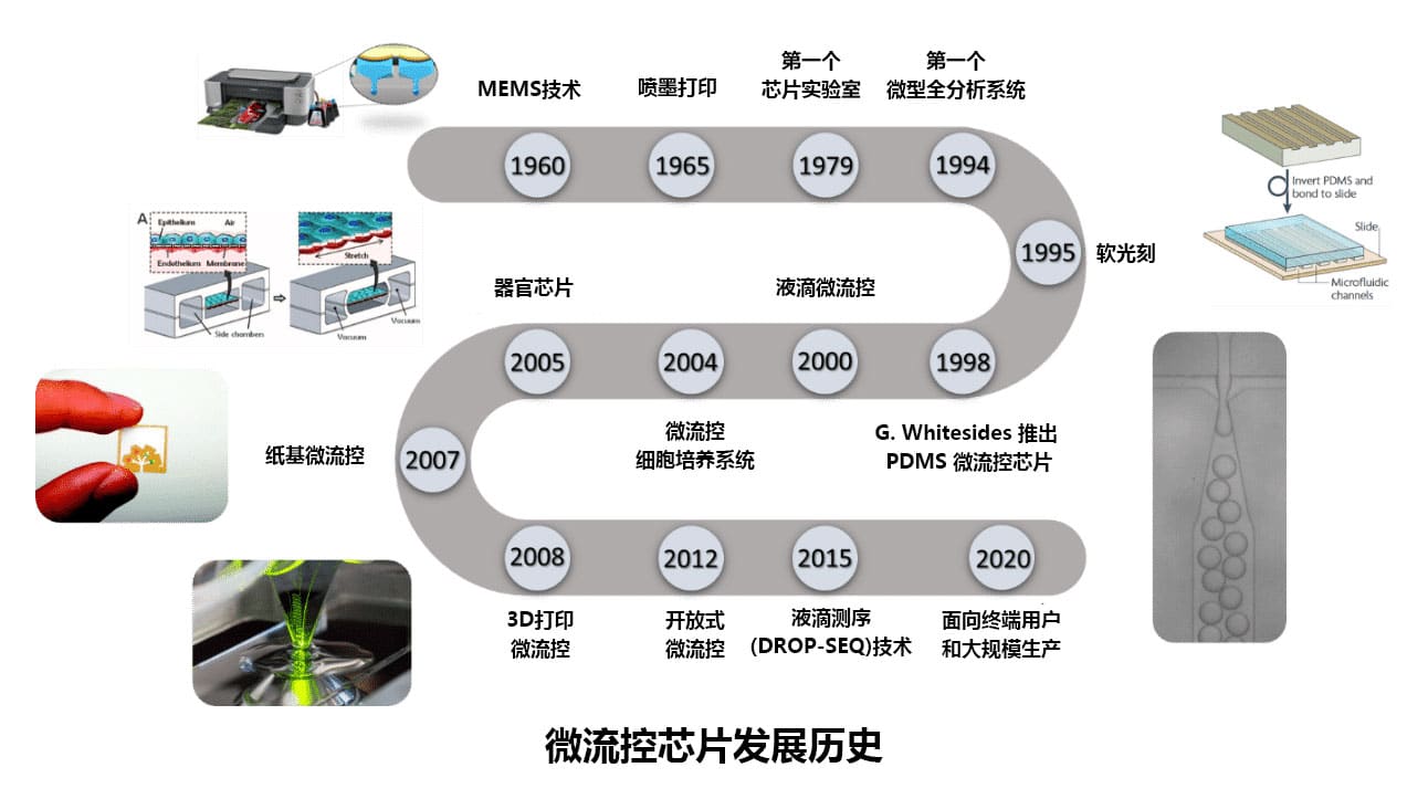
History of microfluidic chip development
Microfluidic chip technology was born in the 1990s, when Manz et al. successfully used microfluidic chip technology to perform in vitro cell electrophoretic separation and achieve the important function of capillary equivalent, predicting the great potential of microfluidic chips in the field of analysis.
In 1995, the U.S. Department of Defense proposed a handheld individual biochemical self-testing equipment program for soldiers, which sparked great interest in microfluidic chips in the international community. After that, more and more experts and scholars believe that microfluidic chips can be developed into an excellent platform for analytical chemistry, and named them "Miniaturized Total Analysis Systems" (μTAS).
In 2000, Mcdonald et al. of Harvard University first proposed a soft lithography method based on PDMS (polydimethylsiloxane) as a process substrate, which greatly simplified the microfluidic chip processing process and greatly contributed to the rapid development of microfluidic chip processing. In the same year, Quake et al. published a paper entitled "Microfluidic Large-Scale Integration" in Science, which integrated thousands of control valves and hundreds of reactors on a single chip and used microvalve and micropump technology to precisely control microfluidic flow. The paper, entitled "Microfluidic Large-Scale Integration", integrated thousands of control valves and hundreds of reactors on a single chip, and used microvalve and micropump technology to precisely control microfluidic flow, which aroused widespread attention and concern among researchers for the application of microfluidic chip technology.
In 2006, Daw et al. published a report entitled "Lab on a Chip" in Nature magazine, which analyzed and explained the development and application of micro and nano flow control chips from various perspectives, and listed LOC as one of the "seven technologies of this century". The report entitled "Lab on a Chip" analyzed and explained the development and application of micro and nano-fluidic chips from various perspectives, and listed LOC as one of the "seven technologies of this century". At this point, the strategic significance of Lab on a Chip has been recognized by both academia and industry at a higher level and in a wider scope.
When the channel size on a micro-nano-fluidic chip is reduced from the micron (µm) to the nanometer (nm) scale, the van der Waals force, electrostatic force, and capillary force inside the channel gradually dominate in the action on the fluid. The combined effect of these forces generates physical phenomena that are different from macroscale and micron fluids, such as interface-related heat transfer and greatly increased surface forces, which have stimulated great interest in nanofluidic chips.
What are the common materials used in microfluidic chips?
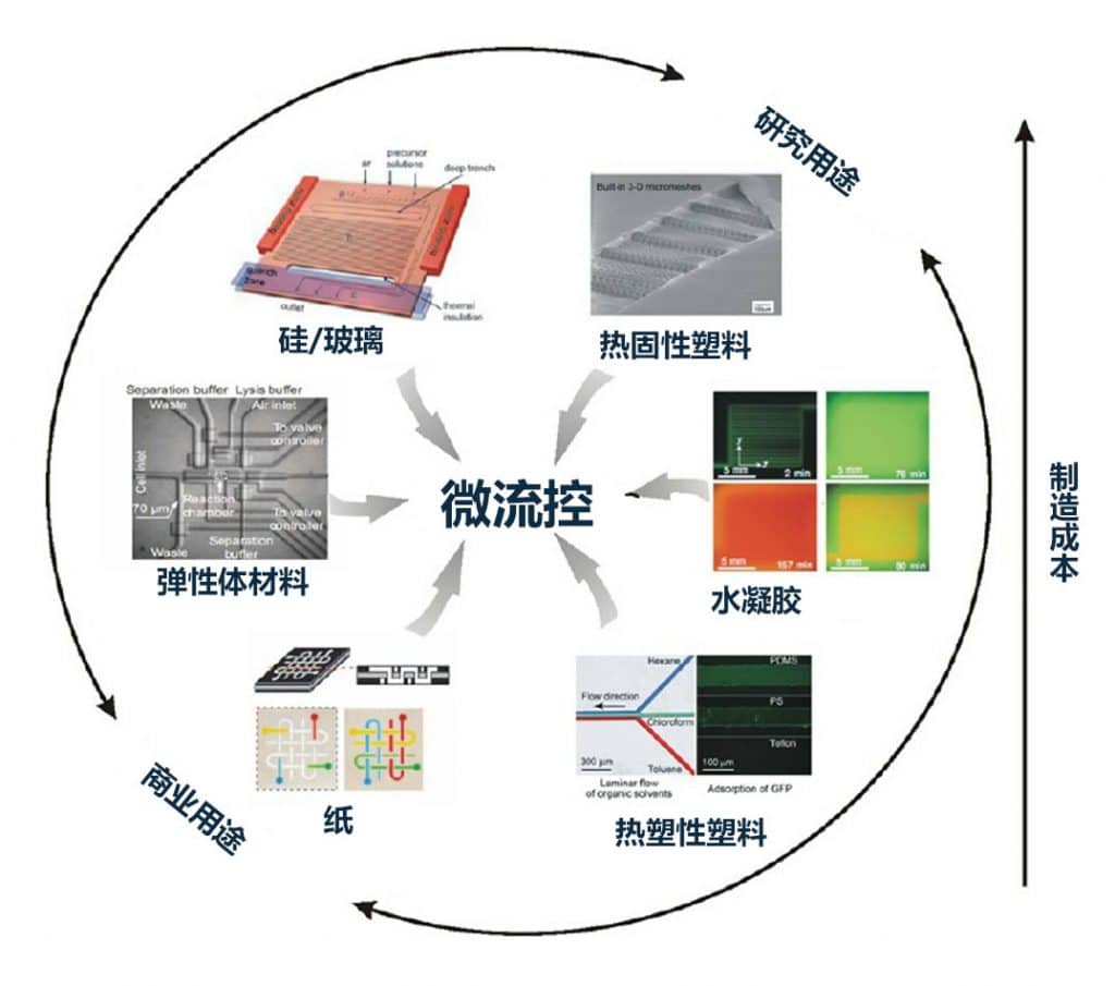
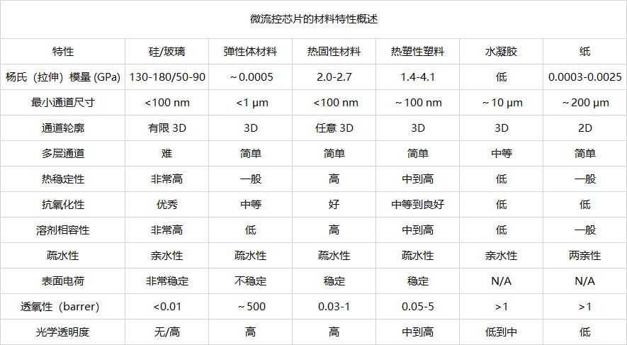
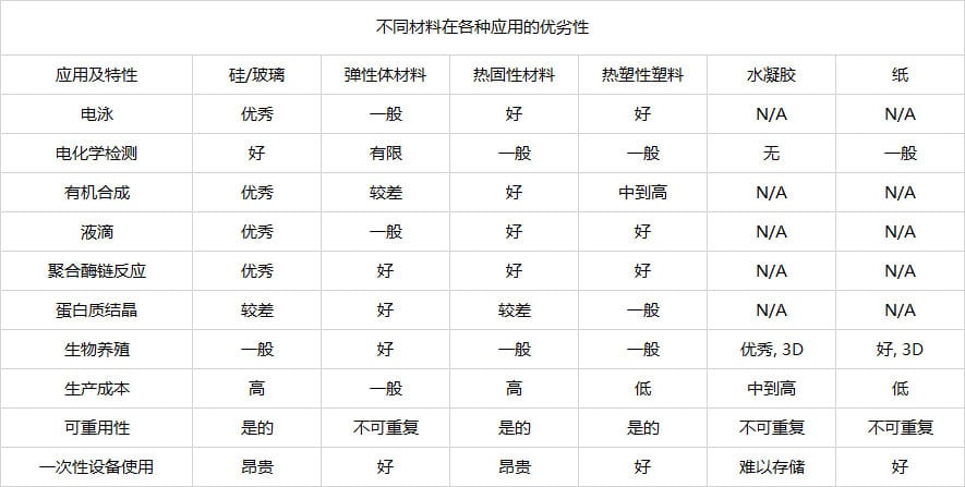
Materials used in the manufacture of microfluidic chips can be divided into three main categories.Inorganic materials, polymers and paper.
Inorganic materials.Silicon, glass, ceramics
Polymers.Elastomers [polydimethylsiloxane (PDMS), thermoset polyester (TPE) microfluidic chips
Thermoplastic polymers [Polystyrene (PS))polycarbonate (PC), polymethyl methacrylate (PMMA), polyethylene glycol diacrylate (PEGDA) ), Perfluorinated compounds(PFEP / PFA / PFPE)Polyurethane (PU))]
Microfluidic chip preparation and processing method
The more common processing methods for microfluidic chip preparation are.
① Screen Printing ② Inkjet printing ③ Ultra-Violet (UV) lithography ④ Electron Beam Lithograph (EBL) ⑤ Proton Beam Writing (PBW)(6) Femtosecond laser two-photon direct writing technology
①Screen printing.As a traditional printing technology, it is low-cost and simple, mainly used in circuit boards, medical devices, clothing and other fields. With the development of microfluidic technology, screen printing has been gradually applied to the preparation of microfluidic chips in order to control its cost for industrial production. The equipment requirements of screen printing technology are not high, thus greatly reducing the production cost of microfluidic chips, and the processing steps are few and repeatable, which is conducive to the industrial batch production of microfluidic chips.
②Inkjet printing.The advantages are high speed, automation, low cost, environmental friendliness, etc. Inkjet technology allows ink droplets to be ejected directly onto the circuit board for precise circuit mapping.
③ Ultraviolet lithography.UV light sources are widely used in high-precision processing because of their short wavelength, high photon energy, and high processing resolution. In the process of UV lithography, the material absorbs a UV photon and jumps from the ground state to the excited state to trigger the subsequent photopolymerization or photolysis reaction. The main features of UV lithography are as follows.
Small heat-affected area: the processing principle of UV lithography is a photochemical reaction principle, which destroys the chemical bonds in the processed material by direct irradiation with high-energy UV photons, thus its heat-affected area is very small or even no heat-affected area.
Processing a wide range of materials: UV source photon energy is high, so it can process some visible and infrared laser can not process materials.
High resolution: The wavelength of UV light source can generally reach 395 nm, so the diffraction limit size is smaller than that of visible light band, and therefore the resolution is high. It can be processed with a precision of 200 nm or less, enabling the acquisition of precise micro and nano structures.
The UV lithography approach can be divided intoUV mask processingandUV direct writing processingThe UV mask process requires a photoresist mask and the UV laser source is a surface light source. UV mask processing requires a photoresist mask and the UV laser source is a surface light source, while UV direct writing processing does not require a photoresist mask.
④ Electron beam and ⑤ proton beam direct writing techniques. E-beam direct writing is a processing technique to obtain structures by direct exposure of a high-energy electron beam on a substrate coated with a photoresist (photoresist). 100 nm nanostructures were reported as early as 1965 using E-beam direct writing. The wavelength of the electron beam is very short, 0.12 nm at an accelerating voltage system of 100 KV, and according to the Abbe diffraction limit theory, the accuracy of direct electron beam writing can reach the order of nanometers.
Electron beam direct writing nanostructures offer many advantages over other conventional nanostructure processing techniques, such as.High resolution, maskless, long depth of focus, and the ability to write arbitrary nanostructures directly through computer control.The main disadvantage of electron beam direct writing is the mutual proximity effect caused by scattering in the substrate and photoresist gel layers that can cause uneven absorbed dose in the exposed region. Plasmon beam direct writing is a nanofabrication technique that directly processes nanostructures by focusing a high-energy plasmon beam into the photoresist. The penetration ability of the plasmon beam is stronger than that of the electron beam, and the spatial dispersion angle of the plasmon beam is also extremely small, so the plasmon beam direct writing can produce nanostructures with high aspect ratio.
(vi) Femtosecond laser two-photon direct writing technology.It is a laser light source based processing method with narrower pulse width and higher peak power than other traditional continuous laser processing technologies, often interacting with the material through nonlinear effects, processing accuracy can reach less than a hundred nanometers, and has good 3D processing capabilities, so it has great advantages in the field of micro and nano manufacturing. The femtosecond laser reaches the inside of the sample material by means of objective convergence, and since the material interacts with the femtosecond laser in a two-photon or multi-photon absorption manner, only the central region of the laser focus interacts with the material, thus breaking the optical diffraction limit and achieving high precision (resolution <100 nm) processing.
We offerMicrofluidic chips / Nanoimprinting / Micro and nanostructure processing design services, Feel free to leave a message to inquire.
Related Products
Related Reading
UV-LIGA Electroforming | Preparation of fine metal mesh panels with large thickness and high porosity
UV-LIGA Electroforming | Manufacturing Metal Array Stencil

