Superlenses (metalenses)
What is a superlens?
Hyperlens is a two-dimensional planar lens structure made of optical elements that focus light on a super-surface. It is touted as one of the top 10 emerging technologies in 2019.
Superlens hasThinner size, ,Lighter weight, ,Lower cost, ,Better imaging, ,Easier integrationThe advantages of the structure are Moreover, the polarization, phase and amplitude of light can be adjusted by adjusting the shape, rotation direction, height and other parameters of the structure.
Micro and nano structures
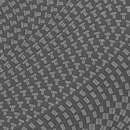
Micro and nano structures
Achromatic Superlens
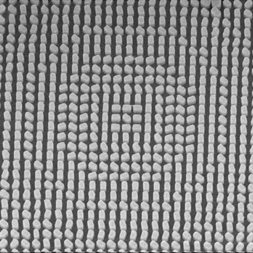
Micro and nano structures
High numerical aperture superlens
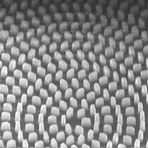
Micro and nano structures
Super-resolution plane superlens
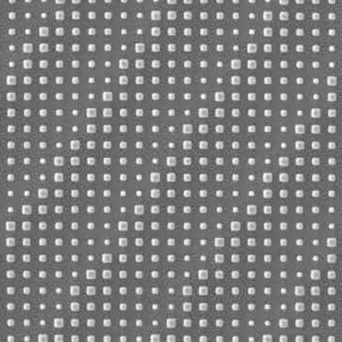
Micro-Nano Architecture
Infrared Superlens
Our Capabilities
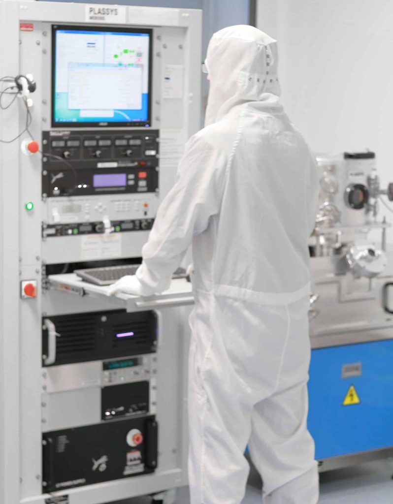
Processes
Lithography (Photolithography)
Electron beam lithography (EBL)UV lithographyProximity/contact lithography, stepper lithography, etc.
Processes
Two-photon 3D printing (Two-photonpolymerization)
Processes
Etching (Etching)
Focused ion beam etching, deep reactive ion etching, inductively coupled plasma etching, ion beam sputtering etching, etc.
Processes
Nanoimprinting(Nanoimprint lithography)
Nano-thermal embossing, UV-curable embossing, micro-contact printing (soft etching)
Processes
Coating
Magnetron sputteringAtomic layer deposition.Ion beam sputtering, ,Plasma chemical vapor deposition, etc.
Processes
Electroforming (LIGA)
Production Process
1. Preliminary offer
Send your drawings and requirements to our development manager for an initial quote
2. Program determination
We will optimize and determine the plan and quotation based on the drawings and requirements
3.Production and quality control
We will select the best equipment for your product and take full responsibility for your product to meet our standards.
4. Delivery on time
Delivered to you on time
Test characterization
Detection means
Optical microscopy (Microscopy)
Detection means
Profilometer (Profilometer)
Detection means
Sheet Resistance Measurement
Detection means
Hall measurement )
Our Advantages
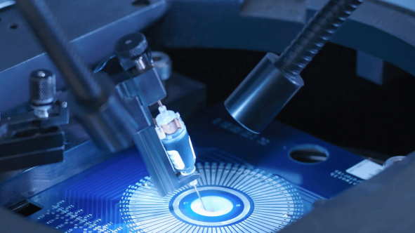
Full process coverage
Cooperate with many domestic experiments and have different processing technology reserve from 100um-5nm
High standard quality control
We adhere to the spirit of 6sigma service, choose the most suitable experimental platform, process, personnel, materials for processing
Quick Response
From idea to implementation, our experts will provide professional advice and ongoingTrackingServices
Save time and worry
Turnkey service, from principle implementation, drawing design, raw material procurement, to finished product processing
Contact Us
Get ready
Did you realize your idea?
You design the future, we build it.
