Micro-Nano Processing | E-paper micro-cup micro-chamber structure preparation
For the current energy crisis, vigorously develop energy-saving and emission reduction technology is an urgent need for the economic model, is expected to become a new generation of environmentally friendly and energy-saving high-tech display products.With the increasingly rapid development of the electronic information industry, integrated circuits, computers, flat panel display industry has become an economic hot spot, the current cathode ray tube display, plasma display, organic electroluminescent display, liquid crystal display and other flat panel display technology to the electronic information industry to add development vitality, to promote the rapid growth of the information industry economy. Electronic paper as a new type of flat panel display technology, due to low energy consumption, flexible and portable and other unique performance, thus the old display industry technology structure a strong impact, promote the flat panel display field of various technologies competition and increasingly perfect.
Electrophoretic display (electronic paper) due to memory characteristics and bistability, thin and portable, flexible and bendable, clear, no backlight, energy saving and other excellent performance, especially the display technology and its products based on the principle of electrophoretic display, microcapsules as the display unit, although in the production process and cost, currently can not be compared with the mature liquid crystal display process, but has triggered a display technology revolution, bringing a huge business opportunities.
Due to the high contrast and reflected light characteristics of electronic paper, it is clearly visible in any strong light, making up for the shortcomings of LCD, thus making cell phones gradually become mini TVs and data terminals, especially solving the problem of unclear displays in tropical countries with strong light intensity. Due to the bistable nature of electrophoretic display technology and the absence of backlight, it has greatly increased the battery life in various mobile devices.
The various technologies currently used to realize electronic paper displays are microcapsules, microcups, electronic powder fluids, toner (toner) displays, rotating spheres, cholesteric liquid crystals, bistable liquid crystals, electrochromic, electrowetting, microelectromechanical, and other microchamber types.
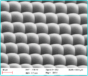
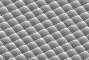
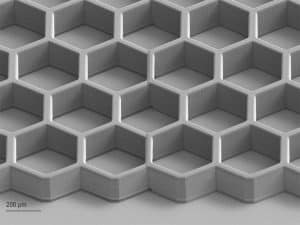
Sipix's microcup structure solves the problems of uneven size, poor mechanical strength, and sensitivity to humidity that exist in microcapsules, and has good mechanical properties and excellent display performance when curled or under pressure; it can be cut to any desired form and size without the use of side sealant, and the liquids in the neighboring areas will not mix with each other or cross-crosstalk during electrophoretic display. sipix's microcup type electronic paper production The process is relatively simple, the cost is relatively low, and it has certain advantages in terms of size, resolution, contrast, response time, full color, and flexibility.
Electronic paper includes display and structure units, and its main technical preparation route methods are as follows.
1. Photolithography
Photolithography is the process of transferring an image from a master plate to another medium under the action of light. Current lithography techniques include conventional lithography, electron beam lithography, ion beam lithography (IPL), theX Ray lithography, extreme ultraviolet lithography (EUL), nano-imprintingetc.
2. Nanoimprinting
Embossing technology also includes thermal embossing (HEL), UV embossing (UV-NIL) and micro-contact printing (μCP) and other technologies are implemented through hot melt molding, UV curing in-mold molding, and contact stamp molding methods.
3. Stencil etching technology
Stencil etching techniques including mask lithography, colloidal lithography, colloidal ion etching, etc..
We offer fastMEMS device / micro and nanostructure processing design services, Feel free to leave a message to inquire.
Related Products
Related Reading
Micro and Nano Processing | 3D Optical Structure Grayscale Lithography
微纳加工 | 三维光学结构灰度光刻 灰度


