Diffractive Optical Elements (DOE)
What is a diffractive optical element
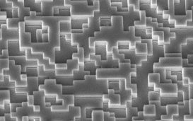
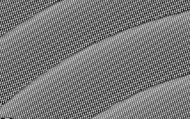
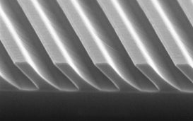
Diffractive Optical Elements (DOE) are phase elements, which are based onThe theory of optical wave diffraction utilizes a continuous relief-type or step-type structure etched on the substrate to obtain extremely high diffraction efficiency.Its small size, light weight, design freedom, imagingGood quality, broad application prospects in the fields of optical imaging, optical data storage, laser technology, biomedicine, etc.
There are three types of functions:Beam shaper, ,Beam splitterandDiffusers(also known as homogenizer)
DOE Application Areas

Laser material processing
Shaping and beam splitting of laser beams in welding, cutting, scribing, soft welding and drilling processes
Applications
Photolithography and holographic illumination
Homogenization of projection beams in mask projection systems, structured pupil illumination, uniform field illumination of vertical and highly inclined planes
Applications
Biomedical Equipment
Diffractive optics for medical laser therapy and diagnostic instruments
Applications
Optical Sensors
Distance and position sensors, motion detection
Applications
LIDAR
Optical distance and speed measurement using laser beams
Applications
Communication
Beam splitters, wavelength selection and silicon optics applications
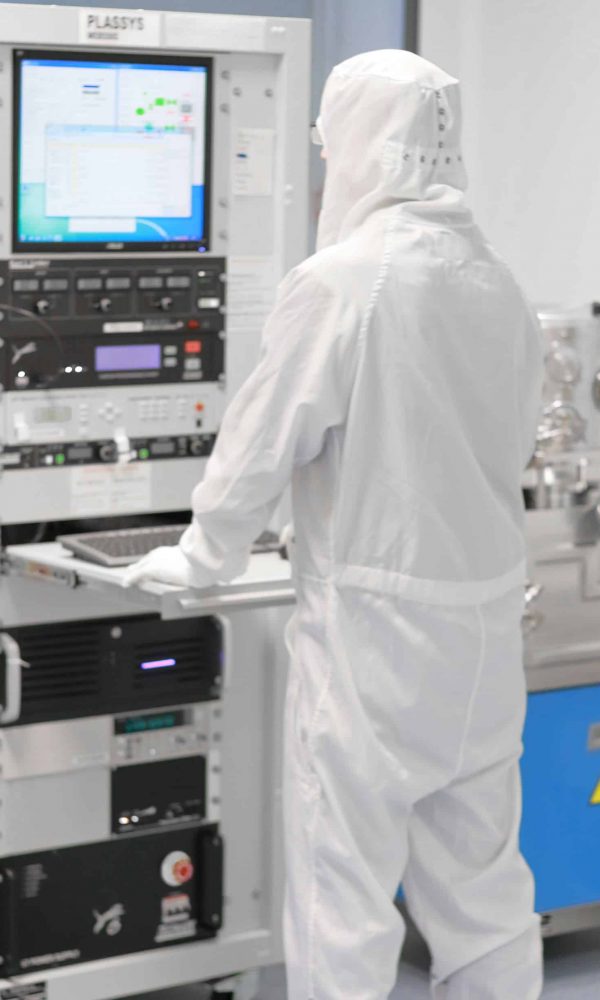
Our Capabilities
Processes
Lithography (Photolithography)
Electron beam lithography (EBL)UV lithographyProximity/contact lithography, stepper lithography, etc.
Processes
Two-photon 3D printing (Two-photonpolymerization)
Processes
Etching (Etching)
Focused Ion Beam EtchingDeep reactive ion etching, inductively coupled plasma etching, ion beam sputtering etching, etc.
Processes
Nanoimprinting(Nanoimprint lithography)
Nano-thermal embossing, UV-curable embossing, micro-contact printing (soft etching)
Processes
Coating
Magnetron sputteringAtomic layer deposition.Ion beam sputtering, ,Plasma chemical vapor deposition, etc.
Processes
Electroforming (LIGA)
Production Process
1. Preliminary offer
Send your drawings and requirements to our development manager for an initial quote
2. Program determination
We will optimize and determine the plan and quotation based on the drawings and requirements
3.Production and quality control
We will select the best equipment for your product and take full responsibility for your product to meet our standards.
4. Delivery on time
Delivered to you on time
Cases we have done
Micro and nano structures
Diffractive Optical Elements (DOE)
Micro and nano structures
Superlenses (METALENSES)
Micro and nano structures
Diffraction grating (line point, shine, tilt)
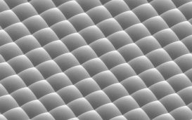
Micro-Nano Architecture
Microlens arrays
Test characterization
Detection means
Optical microscopy (Microscopy)
Detection means
Profilometer (Profilometer)
Detection means
Sheet Resistance Measurement
Detection means
Hall measurement )
Our Advantages
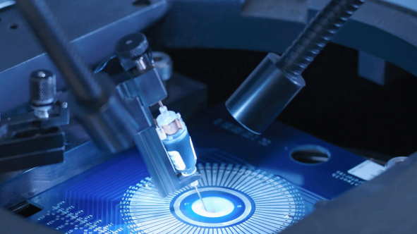
Full process coverage
Cooperate with many domestic experiments and have different processing technology reserve from 100um-5nm
High standard quality control
We adhere to the spirit of 6sigma service, choose the most suitable experimental platform, process, personnel, materials for processing
Quick Response
From idea to implementation, our experts will provide professional advice and ongoingTrackingServices
Save time and worry
Turnkey service, from principle implementation, drawing design, raw material procurement, to finished product processing
Contact Us
Get ready
Did you realize your idea?
You design the future, we build it.

